High-Purity Titanium Sputtering Target & Thin-Film Materials
Engineered for semiconductor interconnects, optical coatings, architectural glass, display panels, and hard wear-resistant PVD applications. Available in 3.5N to 5N purity, custom planar, and high-yield rotary geometries.
High-Performance Titanium Sputtering Target Classifications
Almerca Titanium Industry Co., Ltd. manufactures a full spectrum of Titanium Sputtering Targets manufactured from high-purity sponge titanium via Vacuum Electron Beam Melting (EB) and Vacuum Arc Remelting (VAR), followed by precision thermo-mechanical processing (TMP) to guarantee microstructural uniformity and low gas content.
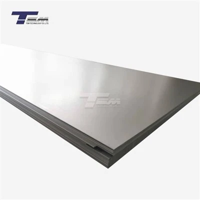
Standard Specification Matrix: Titanium Sputtering Target
| Purity Grade | Ti Content (%) | Impurity Limits (ppm max) | Typical Applications | Available Forms |
|---|---|---|---|---|
| 3.5N (Industrial) | 99.95% | Fe < 150, O < 300, N < 50, C < 50, H < 20 | Decorative PVD coatings, watch cases, door hardware, automotive trim | Planar Discs, Plates, Tiles |
| 4N (Optical/Display) | 99.99% | Fe < 30, O < 150, N < 20, C < 20, H < 10 | TFT-LCD display electrodes, optical anti-reflective coatings, Low-E glass | Planar Rectangular, Rotary Tubes |
| 4.5N (Advanced Optics) | 99.995% | Fe < 10, O < 100, N < 10, C < 10, H < 5 | Touch panel sensors, thin-film solar cell back-contact metallization | Planar, Rotary Monolithic |
| 5N (Semiconductor) | 99.999% | Fe < 1, Ni < 1, Cr < 1, Cu < 1, Na < 0.5, K < 0.5 | VLSI interconnects, barrier layers (Ti/TiN), EUV mask blanks, microelectronics | High-Precision Custom Planar |
How Microstructure & Bonding Integrity Determine Deposition Quality
1. Grain Size Refinement & Texture Control (0002 Crystallographic Orientation)
In physical vapor deposition (PVD), the sputtering rate of titanium atoms is strongly directional. A coarse-grained titanium target with random crystallographic orientations causes uneven erosion tracks, local micro-arcs, particle flaking, and severe thin-film thickness variations across the wafer or glass substrate.
At Almerca Titanium Industry Co., Ltd., we utilize multi-axis forge rolling combined with strictly controlled recrystallization annealing. This proprietary thermo-mechanical treatment controls the average titanium grain size to under 50 micrometers (<50 μm) with an equiaxed grain distribution. Furthermore, we optimize the crystallographic texture toward preferred (0002) hexagonal close-packed (HCP) orientations, boosting sputtering efficiency by up to 18% while suppressing target arcing.
Future Procurement Trends & Technology Roadmap for Titanium Targets
Transition to Ultra-Long Rotary Targets in Architectural Glass
Global glass coaters are rapidly replacing traditional planar targets with continuous rotary titanium targets up to 3.8 meters in length. The shift is driven by the demand for double and triple-silver Low-E energy-efficient coatings, where rotary targets dramatically reduce system downtime, improve coating uniformity, and lower total cost of ownership (TCO).
Ultra-High Purity (5N5) Demand in Sub-3nm Semiconductor Nodes
As chipmakers advance toward 2nm and 1.4nm semiconductor fabrication, trace alkali metallic contaminants (Na, K, Li > 0.1 ppm) and heavy metals (U, Th > 1 ppb) in titanium barrier films become fatal to device yield. Sourcing 5N to 5N5 grade titanium targets evaluated via Glow Discharge Mass Spectrometry (GDMS) is becoming a strict procurement baseline.
Perovskite-Silicon Tandem Photovoltaic Metallization
Next-generation solar module manufacturing relies heavily on titanium sputtering targets to deposit ultrathin transparent conductive oxide (TCO) buffer layers and corrosion-resistant back contacts. Demand for customized Ti-Al alloy targets and high-density pure Ti targets in the solar sector is projected to grow at a CAGR of 16.4% through 2030.
Almerca Titanium Manufacturing Capabilities & Quality Assurance
Vertically Integrated Production: Smelting to Precision Machining
Almerca Titanium Industry Co., Ltd. operates 3 modern manufacturing bases spanning over 60,000 m² in Shaanxi Province, China — the hub of global titanium material science. Our integrated facility houses over 100 sets of advanced processing equipment, including Vacuum Electron Beam Smelting furnaces, 10,000-ton hydraulic forging presses, high-precision CNC vertical lathes, and Class 10,000 cleanroom bonding stations.